

Introduction
Photoresist dry film plays an important role in PCB circuit pattern formation. Its performance affects pattern transfer, plating, etching, and final circuit quality.
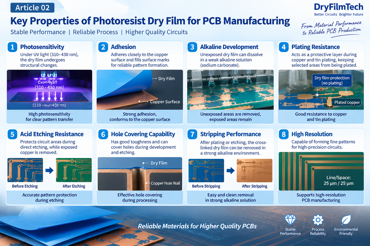
Photosensitivity
Photosensitivity refers to the ability of dry film to undergo structural changes when exposed to a specific wavelength of light. Stable photosensitivity supports clear and consistent pattern transfer.
Adhesion
Dry film needs to adhere closely to the copper surface. Good adhesion allows the film to conform to the copper surface and fill surface marks created during previous processing.
Alkaline Development
Unexposed dry film can dissolve in a weak alkaline sodium carbonate solution. During development, the unexposed portion is removed while the exposed portion remains.
Plating Resistance
Dry film can act as a protective layer during copper and tin plating, protecting selected areas while allowing exposed copper areas to undergo plating.
Acid Etching Resistance
For direct etching, dry film protects circuit areas that should remain while exposed copper is removed.
Hole Covering Capability
Dry film has a degree of toughness and can provide hole-covering capability during development and etching.
Stripping Performance
After plating or etching, the cross-linked dry film needs to be removed in a strong alkaline environment. Reliable stripping supports clean downstream processing.
High Resolution
High-resolution dry film can form fine circuit patterns, helping PCB manufacturers meet the requirements of high-precision circuit production.
Conclusion
Dry film performance should be evaluated as a combination of photosensitivity, adhesion, resolution, process resistance, and stripping behavior.