

What Is Photoresist Dry Film?
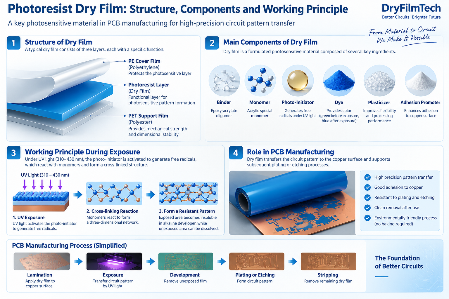
Photoresist dry film is a photosensitive material used in PCB manufacturing to transfer circuit patterns onto a copper surface. Through exposure and development, the dry film forms a protective pattern that supports subsequent plating or etching processes.
Structure of Dry Film
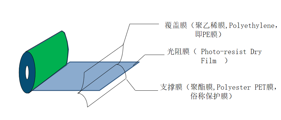
A typical dry film structure consists of three main layers:
- Polyethylene (PE) cover film
- Photoresist dry film layer
- Polyester (PET) support film
The photoresist layer is the functional layer responsible for photosensitive pattern formation.
Main Components of Dry Film
- Binder: Epoxy-acrylate oligomer
- Monomer: Acrylic special monomer
- Photo-initiator
- Dye
- Plasticizer
- Adhesion promoter
How Does Dry Film React During Exposure?
During exposure, ultraviolet light activates the photo-initiator in the photoresist layer. The training material describes an exposure wavelength range of approximately 310–430 nm. The activated photo-initiator produces free radicals, which react with monomers and initiate a cross-linking reaction.
The photoresist changes from a linear structure into a three-dimensional cross-linked structure. The exposed area becomes resistant to the alkaline development solution, allowing the desired circuit pattern to remain after development.
Why Is Dry Film Important in PCB Manufacturing?
The basic sequence can be summarized as:
Lamination → Exposure → Development → Plating or Etching → Stripping
Conclusion
Understanding dry film structure and its reaction mechanism is the foundation for understanding PCB dry film processing. Stable results depend on the material and on controlled lamination, exposure, development, and subsequent processes.